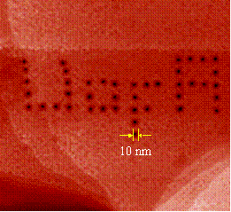
FAYETTEVILLE, Ark. — The world of nano-machines has moved a step closer to reality, thanks to researchers who have found a way to sculpt material at the nanoscale in a predictable, controllable and inexpensive manner by using a conducting liquid medium.
This technique has potential applications in single DNA detection devices such as nanopores, nanoscale interconnects in biological and semiconducting devices, molecular sieves for protein sorting and nanojets for fuel or drug delivery.
Ajay Malshe, associate professor in mechanical engineering at the University of Arkansas; K. Virwani and Devesh Deshpaned, student researchers; and K.P. Rajurkar of the University of Nebraska, Lincoln, are presenting their results at the meeting of the International Institution for Production Engineering Research. They also will publish their manuscript in the institution’s journal.
“With this technique, you can remove on demand precisely what you want to, where you want to remove it,” Malshe said. “It’s very simple but very powerful.”
The researchers use a technique called nanoscale electro-machining (nano-EM) to etch nanopores as small as 8-10 nanometers in diameter on an atomically flat gold surface.
They used a scanning tunneling microscope with a platinum-iridium atomically sharp electrode tool dipped in a dielectric oil medium to apply an electric field to the system. The tool and the surface remain about two nanometers apart. As a voltage passes through the system, the tunneling electrons move between the tool and the surface through the oil’s molecules and cause precise ejection of gold atoms, which creates the tiny pores.
Currently, creating a nanopore by the standard scanning tunneling microscopy techniques requires vacuum chambers and expensive equipment. And frequently the samples must be transferred from the machine that created them to a different instrument that can examine them, which takes time and money. Both of these issues pose a problem for manufacturers who might be interested in developing nanoscale electronic, biomedical and other related products.
With nano-EM, the liquid medium allows researchers to work outside of the expensive vacuum environment, and it is responsible for the precision because of the long chain molecules found in the oil. The current process becomes unpredictable when performed in ambient air, but introduction of oil as a medium made a dramatic difference in both precision and reproducibility.
“Researchers believe that long chain oil molecules are acting as 'nano-wires’ to connect the nano-EM tool tip and the substrate for precise application of the intense field,” Malshe said. “Every molecule between the tiny gap of two to three nanometers is acting as a conductive wire.”
The researchers designed the system so that the scanning tunneling microscope alternates between acting as the machining system and the probe. This technique has enabled the researchers to create nanopores on the surface and see the images at the same time — an important advantage in nano-manufacturing, because it means scientists can create a nano-well and immediately determine whether or not it has the correct atomic scale dimensions. This eliminates the problem of having to transport a sample to another detection device to ensure its quality.
“This is one of the few techniques that allows you to 'write’ and 'read’ at the same time,” Malshe said.
This also is one of the few techniques that allows researchers to manipulate various materials -- from silicon to silicon nitride to gold -- by the selection of appropriate liquid and process conditions. The process can be used with computer-aided designing (CAD) systems for automation and can be scaled up for mass production.
Eventually, the researchers hope this technique will allow scientists to work at the nanoscale with all kinds of conducting and semi-conducting materials in a non-vacuum, cost-saving environment.
The researchers have patents pending in this area. To bring the benefits of the technology to the user community, the university is licensing the patent rights to NanoMech LLC, based in the Innovation Center at the University of Arkansas Research & Technology Park. Malshe is the company's co-founder and chief technology officer.
“Our long-term goal is to create a complete nanofabrication laboratory on a microchip — machining, deposition, metrology and assembly events at nanoscale, at a given time, at a given place and according to engineering specifications,” Malshe said.
Contacts
,